WONACH SUCHST DU?
Einführung
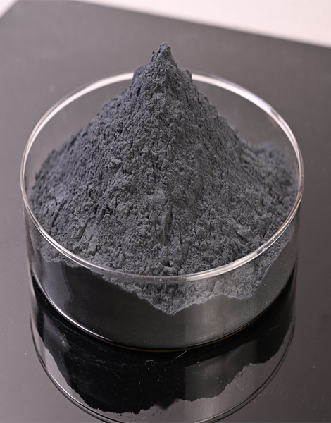
Bor dient als zentrales p-Dotiermittel in der Halbleiterfertigung für das Wachstum von CZ-Einkristall-Silizium, Ionenimplantation und Diffusionsprozesse. Die Bor-Dosierung beeinflusst direkt die elektrischen Eigenschaften der Bauelemente. Die Wahl zwischen 4N (99,99 %) und 6N (99,9999 %) Bor ist eine wichtige Entscheidung für Ingenieure und Supply-Chain-Manager. Dieser technische Leitfaden analysiert die Kontrolle von Verunreinigungen, Gitterdefekten, Testmethoden und die Gesamtbetriebskosten und bietet Kunden somit eine praxisnahe Orientierung.
I. Definition von Reinheit: Mehr als nur Prozentzahl, ein deutlicher Unterschied bei den Verunreinigungen
Obwohl sich 4N und 6N nur durch zwei zusätzliche „9“ unterscheiden, variieren ihre Gesamtverunreinigungsgrade um zwei Größenordnungen (das Hundertfache):
| Grad | Reinheit | Gesamtgehalt an Verunreinigungen | Typische Anwendungsszenarien |
| 4N | 99,99 % | ≤ 100 ppm | PV-Silizium, industrielle Halbleiter, Legierungszusätze |
| 6N | 99,9999 % | ≤ 1 ppm | IGBT/MOSFET-Leistungshalbleiter, fortschrittliche Ionenimplantation, 12-Zoll-Wafer |
Ein weit verbreiteter Irrtum: Ein ausreichender Boranteil allein qualifiziert ein Material für Halbleiter. Tatsächlich dringen Spuren metallischer und nichtmetallischer Verunreinigungen im ppm- oder ppb-Bereich während Hochtemperaturprozessen in das Siliziumgitter ein und bilden Ladungsträgerfallen. Dies kann zu einer Drift der Schwellenspannung, einem erhöhten Leckstrom oder sogar zum vollständigen Wafer-Verwerfen führen.
II. Drei Kernmechanismen, wie sich die Reinheit auf die Dopingleistung auswirkt
1. Lebensdauer von Übergangsmetallen und Minoritätsträgern
4N-Bor enthält Dutzende ppm Restmengen an Fe, Cu, Ni und anderen Übergangsmetallen, die beim Kristallziehen oder Diffusionsprozess tiefe Defektniveaus bilden, Ladungsträger einfangen und die Lebensdauer der Minoritätsladungsträger drastisch verkürzen. 6N-Bor begrenzt den Gehalt an Übergangsmetallen streng auf unter 0,1 ppm, um Rekombinationszentren zu reduzieren und eine überlegene elektrische Leistung zu gewährleisten.
2. Kohlenstoffverunreinigung – Die unterschätzte, versteckte Gefahr
Kohlenstoff besitzt eine hohe Affinität zu Bor; selbst 6N β-rhomboedrisches Bor enthält 30–60 ppm Kohlenstoff. Dies hat zwei Konsequenzen:
Für Lieferanten: Die Behauptung, kohlenstofffreies 6N-Bor zu liefern, ist unwissenschaftlich; es müssen spezifische Kohlenstoff-Testdaten vorgelegt werden.
Für Verfahrenstechniker: Kohlenstoff kann Bor bei hohen Temperaturen deaktivieren, was Anpassungen der Glühtemperatur und -dauer innerhalb der Prozessfenster erforderlich macht.
3. Prozesskonsistenz und thermische Stabilität
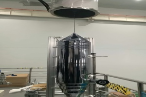
Hohe Kohlenstoff- und Sauerstoffverunreinigungen in 4N-Bor führen leicht zur Bildung von Mikropräzipitaten, die Versetzungen und Stapelfehler in Siliziumkristallen verursachen und den Leckstrom erhöhen. Niedrigschmelzende Verunreinigungen verdampfen oberhalb von 2000 °C, kontaminieren die Öfen und verursachen Dotierungsschwankungen. 6-Bor zeichnet sich durch eine ausgezeichnete thermische Stabilität aus, die präzise Dotierungskonzentrationsprofile und einen gleichmäßigen Flächenwiderstand ermöglicht – entscheidend für die Ausbeute in der Massenproduktion.
III. Verborgene Diskrepanzen hinter Reinheitsangaben – Testmethodik
Dies wird von Käufern leicht übersehen: Identische Proben können bei unterschiedlichen Testverfahren drastisch unterschiedliche Reinheitsbewertungen erhalten.
ICP-MS detektiert typischerweise etwa 15 Verunreinigungselemente
GDMS analysiert Feststoffproben direkt und identifiziert bis zu 70 Verunreinigungen; es gilt als Goldstandard für die Spurenanalyse von hochreinen Materialien.
Ein Material, das mittels ICP-MS mit 6N bewertet wird, kann unter GDMS aufgrund einer umfassenderen Verunreinigungserkennung und nicht aufgrund von Veränderungen im Material selbst nur als 4N eingestuft werden.
Praktische Empfehlungen für Käufer
* Lieferanten müssen die Testmethoden und die Anzahl der nachgewiesenen Elemente klar angeben.
* Bitte fordern Sie vollständige Elementverunreinigungslisten mit ppm/ppb-Werten anstelle von nur Gesamtreinheitsprozenten an.
* GDMS-geprüftes 6N-Bor sollte für Anwendungen in fortgeschrittenen Knoten priorisiert werden.
IV. Anwendungsgrenzen von 4N- und 6N-Bor
| Vergleichsartikel | 4N Bor (99,99 %) | 6N Bor (99,9999 %) |
| Gesamtverunreinigungen | ≤ 100 ppm | ≤ 1 ppm; wichtige Verunreinigungen im ppb-Bereich |
| Anwendbare Szenarien | PV-Silizium, verschleißfeste Keramik, einfache diskrete Bauelemente, metallurgische Modifikation | 8–12 Zoll große p-dotierte Silizium-Einkristalle, IGBT/MOSFET, fortschrittliche epitaktische Dotierung, Quantenbauelemente |
| Prozessrisiken | Widerstandsschwankungen, hoher Leckstrom, Ofenverschmutzung | Extrem geringes Risiko, hervorragende elektrische Konsistenz |
| Kostenpositionierung | Wirtschaftliche Qualität | Hochwertige Elektronikqualität mit überlegenen Gesamtausbeutekosten |
5N (99,999%) Bor kann als Kompromiss für diskrete Bauelemente mittlerer Größenordnung oder für Übergangsprozesse in Betracht gezogen werden.

V. Gesamtbetriebskostenperspektive (TCO) für die Auswahl
Obwohl 6N-Bor höhere Anschaffungskosten verursacht, bietet es Vorteile hinsichtlich der gesamten Herstellungskosten:
* Reduzierung des Wafer-Ausschusses: Die Kosten eines einzelnen Chargenfehlers aufgrund übermäßiger Verunreinigungen übersteigen die Materialpreisdifferenzen bei weitem.
* Reduzierung versteckter Gemeinkosten: Widerstandsdrift bei 4N-Bor erfordert zusätzliche Tests und Prozessoptimierung.
* Verlängerung der Anlagenlebensdauer: Flüchtige niedrigschmelzende Verunreinigungen erhöhen die Reinigungsfrequenz des Ofens und führen zu Ausfallzeiten und Verlusten.
* Steigerung der Produktpräferenz: Mit 6N-Bor dotierte Wafer und Chips zeichnen sich durch eine lange Minoritätsträgerlebensdauer und geringe Leckströme aus und ermöglichen so eine stärkere Preissetzungsmacht in High-End-Märkten.
Auswahllogik
Wählen Sie 4N-Bor für kostensensible Anwendungen mit hoher Prozesstoleranz; verwenden Sie 6N-Bor für Produkte mit hoher Ausbeute und hoher Konsistenz, die auf Premiummärkte abzielen; evaluieren Sie 5N-Bor für Prozesse der mittleren Preisklasse.
VI. Markttrend: Streben nach höherer Reinheit
Mit der Miniaturisierung von Halbleiterbauelementen steigen die Anforderungen an die Reinheit kontinuierlich. Die Nachfrage nach 5N- und 6N-Reinheitsbor steigt mit der zunehmenden Verbreitung fortschrittlicher Fertigungsprozesse sprunghaft an. Hochreine Borquellen werden daher für die zukünftige High-End-Halbleiterfertigung unerlässlich sein.
VII. Hochreine Borlösungen von BoronHub
Als professioneller Lieferant von borbasierten Hochleistungsmaterialien liefert BoronHub elementares Borpulver, kristalline Granulate und Borverbindungen bis zu einer Reinheit von 6N (99,9999 %):
• Strenge Prüfungen: Jede Charge wird einer GDMS- und ICP-MS-Analyse unterzogen, die 70 Verunreinigungen abdeckt, inklusive vollständigem Analysezertifikat und detaillierten Daten zum Kohlenstoffgehalt.
Anpassbare Morphologie: Pulver-, Granulat- und Blockformen, maßgeschneidert für Kristallzieh-, Diffusions-, Ionenimplantations- und Verdampfungsprozesse
Unterstützung bei der Einhaltung von Vorschriften: Hilfe bei der Erstellung von Dokumenten zur Einhaltung der Endbenutzer-Zertifizierungsvorschriften (EUC).
Egal ob Sie ein etablierter Halbleiterhersteller oder ein Entwickler von Spitzentechnologien sind, BoronHub bietet zuverlässige Reinheit und professionellen technischen Support, um die Produktionsausbeute und die Wettbewerbsfähigkeit Ihrer Produkte zu steigern.
Abschluss
Die beiden zusätzlichen „9“ zwischen 4N- und 6N-Bor symbolisieren Generationsunterschiede bei der Reinigung, der Kontrolle von Verunreinigungen und den Teststandards. Die Dotierung von Halbleitern erfordert Präzision auf atomarer Ebene; selbst kleinste Abweichungen bei den Verunreinigungen im Rohmaterial wirken sich auf fertige Chips drastisch aus. Bei der Auswahl des Reinheitsgrades geht es nicht einfach darum, die höchstmögliche Qualität zu erreichen, sondern ein optimales Gleichgewicht zwischen Kosten, Prozessfenster und Produktpositionierung zu finden.
BoronHub – Ihr zuverlässiger Partner für hochreines Bor in der Halbleiterfertigung
Um TDS-Daten, CoA-Daten für hochreines 6N-Bor zu erhalten oder Testmuster anzufordern, wenden Sie sich bitte an unser Team von Halbleitermaterialspezialisten.
Scannen Sie den QR-Code zu WeChat :

Scannen und zu WhatsApp senden :

Heim
Produkte
Kontaktieren Sie uns